


(Nov 16): SK Hynix Inc plans to open a semiconductor testing facility next year in partnership with the Korean government, angling to boost the global competitiveness of the country’s smaller chip equipment makers.
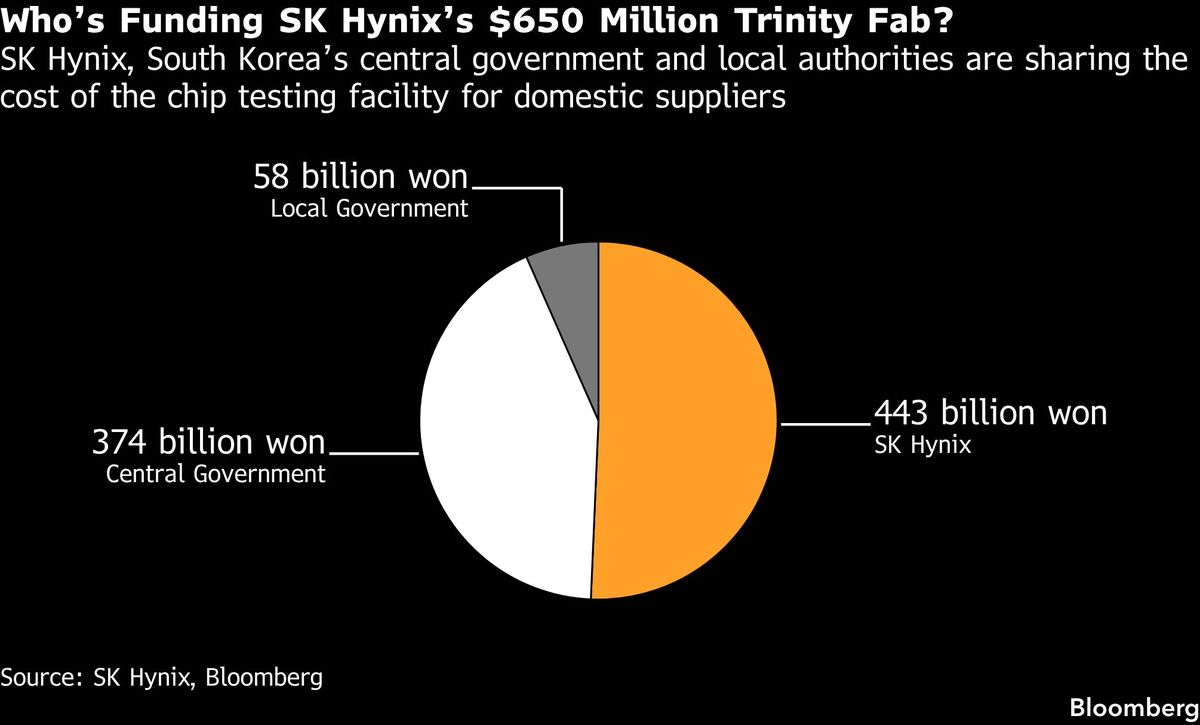
The 874.6 billion won (US$654 million) facility is being built inside the sprawling Yongin Semiconductor Cluster, which is under construction south of Seoul, SK Hynix said in a statement on Monday. The Trinity Fab facility will open in May with equipment that small and medium-sized suppliers can use to conduct final performance and yield validation before their products are deployed in commercial chipmaking lines, it said.
SK Hynix and homegrown rival Samsung Electronics Co have enjoyed an unprecedented run-up in prices because of a chip scarcity that’s squeezed industries from autos to smartphones. The company is working with the Korean government to eliminate a critical hurdle in the country’s supply chain that has required access to expensive manufacturing infrastructure.
The facility is being jointly financed by SK Hynix, the central government and local authorities, the company said. It will house about 50 pieces of equipment for lithography, etching, deposition, cleaning and measurement, allowing suppliers to test products on 12-inch wafers under conditions resembling those of commercial chip production.
The initiative aims to address a longstanding bottleneck for Korea’s semiconductor supply chain. Smaller materials and equipment makers often face steep costs and lengthy delays in securing access to production-scale testing facilities, making it difficult to demonstrate that their technologies meet the stringent performance and yield requirements of advanced chip manufacturing.
Unlike conventional research laboratories and pilot lines, Trinity Fab will be the world’s first open-access testing facility specifically designed to validate commercial manufacturing readiness for mass production, according to SK Hynix. An independent nonprofit foundation will operate the center to safeguard participants’ intellectual property.
In August, SK Hynix said it would spend US$38 billion to expand its local chipmaking facilities, including a new DRAM manufacturing facility in Yongin and a NAND fabrication plant in Cheongju. The move, covering both dynamic memory for the lowest latency and solid-state storage for fast access to greater quantities of data, is in response to growing demand for memory in the AI era, the company said at the time.
Uploaded by Liza Shireen Koshy