

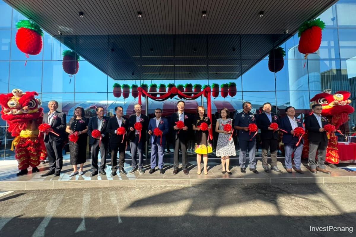
KUALA LUMPUR (Feb 9): Chipbond Technology Corp, a leading global provider of semiconductor packaging and testing services, has opened a new advanced semiconductor packaging and testing facility in Penang. This US$200 million (about RM800 million) investment is part of the group's global expansion strategy.
Located in Valdor Industrial Park, Batu Kawan, the plant is designed to strengthen Malaysia’s position in the global outsourced semiconductor assembly and test (OSAT) value chain.
Malaysian Investment Development Authority (Mida) chief executive officer Datuk Sikh Shamsul Ibrahim Sikh Abdul Majid said the facility would expand Malaysia’s OSAT capacity and ecosystem, while supporting technology transfer and local capability building that will benefit Malaysia’s semiconductor ecosystem for years to come.
“Chipbond is bringing advanced OSAT expertise in wafer bumping and chip-scale packaging that requires highly skilled engineers. With companies like Chipbond anchoring advanced capabilities here, Malaysia is building an integrated semiconductor ecosystem where local talent and SMEs can participate meaningfully in global value chains,” he said in a joint statement from MIDA, InvestPenang and Chipbond.
InvestPenang chief executive officer Datuk Loo Lee Lian, representing Penang Chief Minister Chow Kon Yeow, said the investment aligns with the National Semiconductor Strategy, driving Penang’s shift towards advanced packaging and innovation-led growth.
“Backed by more than 50 years of industrialisation and strong foundation in OSAT, Penang has built a mature ecosystem, a skilled talent base and a conducive business environment,” Loo noted.
“We look forward to seeing strong knowledge transfer, talent upskilling, and deeper collaboration, further strengthening Penang’s position as a regional hub for advanced semiconductor packaging,” Loo added.
Chipbond chairman Wu Fei Jain said the new facility reflects the group’s commitment to expanding its global footprint and ensuring a stable supply chain for its customers.
The Penang plant will offer advanced semiconductor processes, including advanced wafer bumping, wafer-level chip-scale packaging (WLSCP) and comprehensive testing, the statement read. The facility boasts an initial monthly capacity of 10,000 wafers and 100 million WLSCP units. It is also equipped to support flip-chip packaging assembly and test, providing flexibility for future technology and customer requirements.
Internal qualification of the facility is expected to be completed by the end of 2025, with customer qualification slated to begin in the first quarter of 2026, the statement further read.