This article first appeared in Digital Edge, The Edge Malaysia Weekly on October 23, 2023 - October 29, 2023
Technology is the lifeblood of the electrical and electronics (E&E) industry, influencing every aspect of product design, production and functionality. Innovative technology pushes the boundaries of what is possible, from the miniaturisation of components to the integration of smart features.
In the semiconductor and E&E industry, staying at the forefront of technological advancements is imperative for companies to remain competitive.
Mimos Bhd president and CEO Dr Iskandar Samad points to four domains in this industry that are seeing a surge of tech innovations: chip design, advanced packaging technology, automated test equipment and wide bandgap semiconductors.
Iskandar and Jaffri Ibrahim, CEO of Collaborative Research in Engineering, Science and Technology (Crest), note areas where Malaysia is developing cutting-edge capabilities on the back of industry and government collaboration and extensive research and development (R&D).
Chip design
Semiconductor chips hold the data needed to use our computers, smartphones, appliances, cameras and cars. Three-nanometre (nm) chips are currently the most advanced, but 2nm nodes are making headlines. Nodes, or process nodes, refer to a semiconductor manufacturing process.
TIME magazine’s Best Inventions of 2022 (a list of groundbreaking inventions) highlights IBM’s 2nm chip. This technology puts 50 billion transistors, each the size of roughly five atoms, on a space no bigger than a fingernail.
IBM’s new chip, essentially a circuit of connected transistors, is much smaller than the eye can detect. Over the years, transistors have shrunk from an initial 10,000nm in 1971 to 5nm in 2020. The Apple MacBook currently has about 16 billion transistors within its total weight of just 3lbs.
“The 2nm chip technology will develop the world’s smallest and most powerful microchip,” observes Iskandar.
IBM forecasts that the use of this chip will generate an average increase of 45% in product performance. This could allow mobile phones to be charged once every four days rather than daily and autonomous cars to make smarter and quicker decisions. Furthermore, electronics that use this technology should be cheaper because smaller transistors should be less expensive to produce and use up to 75% less energy.
IBM is currently working with manufacturing partners in the US and abroad to begin mass production of 2nm semiconductors in 2024. Meanwhile, Samsung Electronics plans to start mass production of the 2nm process for mobile applications in 2025, high-performance computing in 2026 and automotive in 2027.
Taiwan Semiconductor Manufacturing Company (TSMC), the world’s largest contract manufacturer of semiconductor chips, has responded with its plans to offer the most advanced semiconductor technology globally. Its next-generation 2nm process technology will be introduced in 2025. Its 2nm technology is expected to provide up to 15% speed improvement over N3E (3nm class nodes) at the same power, up to 30% power reduction at the same speed and a chip density of over 15% greater than N3E.
Intel, one of the world’s largest chipmakers, has said it will officially leave nanometre-scale process nodes behind and start classifying chips with angstroms. An angstrom is 0.1nm but Intel’s naming is not based on size. The first chip, expected to launch in the second half of 2024, will be classed as an Intel 20Å node. Intel 20Å is a rebranding of Intel’s 5nm node. This will be followed by Intel 18Å in 2025. Industry observers say these are 5nm nodes with the “equivalent” of 2nm technology.
Advanced packaging technology
Artificial intelligence (AI) advancements are driving a new era in advanced packaging technology. Three-dimensional chip packaging, also known as 3D packaging or 3D integration, is an advanced semiconductor packaging technology that involves vertically stacking multiple integrated circuits or chips on each other within a single package.
In the past, chip packaging was seen as less technologically demanding than the front-end process of designing and fabricating semiconductor wafers. However, advanced packaging, introduced around 2000, started to gain attention as a way to improve chip performance further.
Applications that require high-performance, low-power chips that can rapidly process massive data, such as 5G, autonomous vehicles, Internet of Things devices, and virtual and augmented reality, will benefit from advanced packaging technology. Nvidia’s H100 GPU, which provides the computing power for the popular ChatGPT AI chatbot, uses TSMC’s advanced packaging process.
Yole Intelligence estimates that the market for advanced chip packaging services reached US$44.3 billion in 2022 and will hit US$78.6 billion (RM371 billion) by 2028, a compound annual growth rate (CAGR) of 10.6%.
In Malaysia, Penang will eventually become Intel’s largest production base for 3D chip packaging. The new factory will be Intel’s first overseas facility and the primary product hub for advanced 3D chip packaging using Intel’s Foveros technology. According to the US chipmaker, Amazon, Cisco and the US government have committed to using this advanced packaging technology.
There are opportunities for local E&E companies to move into the advanced packaging space.
“Advanced packaging used to be mundane work, but now it’s becoming essential globally. We have some excellent E&E companies in the country and they will require capabilities in this area. The geopolitical landscape is such that companies are looking for alternative places to build new semiconductor production facilities worldwide.
“These facilities will range from low- to high-end capabilities but will require some element of advanced packaging. While the local industry is unlikely to claim technological dominance, we must be ready to do some advanced packaging work,” says Jaffri.
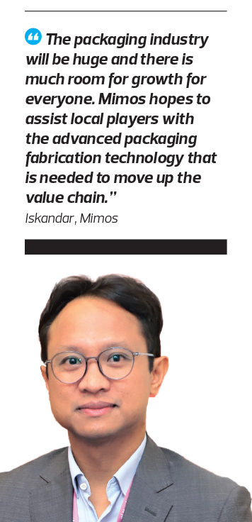
“There is room for manufacturers to add value if they look at co-developing advanced packaging solutions. Some local companies are currently doing flip-chip packaging, so the challenge is to meet the next transitional shift. The packaging industry will be huge and there is much room for growth for everyone. Mimos hopes to assist local players with the advanced packaging fabrication technology that is needed to move up the value chain,” Iskandar says.
Advance packaging is an area that Mimos and Crest’s R&D activities have been focusing on. Crest has identified advanced materials and packaging as a technology cluster. This means the centre actively explores opportunities and fosters new areas of expertise and collaboration in this technology.
Automated test equipment
Another area where Mimos’ Iskandar sees opportunities for the local E&E industry is automated test equipment (ATE). The global ATE market serves diverse industry verticals from consumer electronics, telecommunications and defence to automotive and healthcare. Global trends such as interest in electric vehicles, implementation of 5G technology, Industry 4.0 and the use of AI are driving the growth of the ATE market.
ATE is used for front-end wafer testing and back-end semiconductor testing. This equipment can reduce a semiconductor manufacturer’s production costs and time, check the performance of electronic devices and prevent faulty devices from entering the market.
Market research firm MarketsGlob says the global semiconductor test equipment market reached US$2,076.5 million in 2022 and is expected to reach US$5,002.2 million in 2029, a CAGR of 3%.
Malaysian companies are already in this space. Locally-listed ATE makers include ViTrox Corp Bhd, Greatech Technology Bhd, Pentamaster Corp Bhd, Mi Technovation Bhd, QES Group Bhd, Aemulus Holdings Bhd, MMS Ventures Bhd, Elsoft Research Bhd and VisDynamics Holdings Bhd.
Greatech and Pentamaster are factory automation solution specialists whose clients include multinational corporations in the semiconductor sector. Generally, local ATE companies are not direct competitors as their products and services fulfil a specific need in the semiconductor industry.
“I think the local ATE manufacturers are a formidable force. Many companies are big-scale industry players and making strides towards developing new capabilities such as proprietary software electronic modules or wafer fabrication equipment,” says Iskandar.
Semiconductor wafer fabrication creates circuits used in E&E devices. Global semiconductor wafer fab equipment manufacturers include Applied Materials, ASML, TSMC, Motorola, Samsung and Lam Research.
Wide-bandgap semiconductors
Malaysia stands a good chance of becoming a prominent wide-bandgap semiconductor production hub on the back of its conducive ecosystem and capabilities.
In early 2022, German semiconductor manufacturer Infineon Technologies announced plans for a third manufacturing line to boost its production of wide-bandgap semiconductors that use silicon carbide (SiC) and gallium nitrate (GaN) as the base materials. Both Sic and GaN are high-performance semiconductor materials used in lighting, household appliances, consumer electronic equipment, energy vehicles, smart grids and military supplies.
According to Transparency Market Research, the global wide-bandgap semiconductor market will increase at a CAGR of 24.6% from 2022 to 2031. At the end of 2023, this market should reach a value of US$9.5 billion.
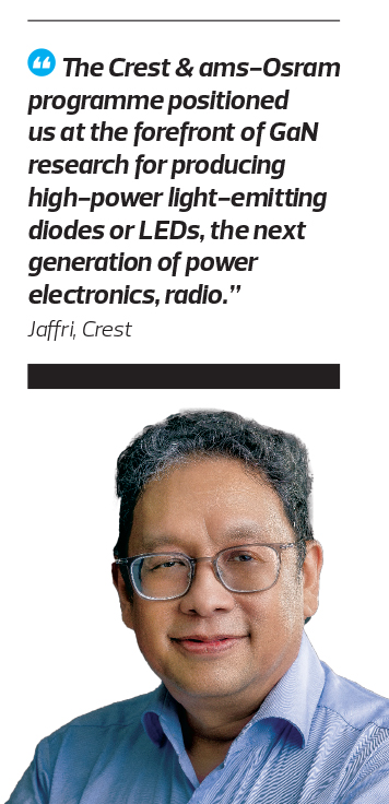
“The country has gained a strong foothold in GaN research and development. One of our greatest hits in collaborative research is in GaN. The Crest & ams-Osram programme positioned us at the forefront of GaN research for producing high-power light-emitting diodes or LEDs, the next generation of power electronics, radio,” says Jaffri.
“When we started this discussion in 2012, we had about a handful of GaN researchers in the country. Now, we have about 80 GaN researchers and companies have decided to invest here because of our capabilities and talent pool,” he adds.
Save by subscribing to us for your print and/or digital copy.
P/S: The Edge is also available on Apple's App Store and Android's Google Play.


