This article first appeared in Digital Edge, The Edge Malaysia Weekly on March 1, 2021 - March 7, 2021
News filtered out less than a month ago that Dagang NeXchange (DNeX) Bhd had won the bid to acquire semiconductor wafer foundry, SilTerra Malaysia Sdn Bhd, from Khazanah Nasional Bhd. However, the foundry is not letting a change in shareholding affect its plans to capitalise on technology trends and play to its strengths.
One of its areas of focus now is the manufacture of sensors, which has seen an upswing in demand with the proliferation of the Internet of Things (IoT), autonomous vehicles and digital health solutions. All these technologies require sensors to collect data from the environment and react to external conditions.
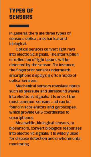
SilTerra senior vice-president of technology development Arjun Kantimahanti points out that there are many different types of sensors available today — chemical sensors, biosensors and mechanical sensors.
Some of these, however, leave much to be desired. “They typically consume a lot of power, so you cannot run them on batteries, and they are bulky and thus difficult to incorporate into anything mobile,” he says.
The semiconductor industry has been challenged to come up with chips that are smaller and consume less power so they can be used in mobile phones, vehicles, factory equipment and medical devices.
This, in turn, has created new opportunities for semiconductor wafer foundries such as SilTerra, which is able to meet the demand for sensors, including those for ultrasound applications, through its micro-electromechanical systems (MEMS)-based piezoelectric micromachined ultrasonic transducers (PMUT).
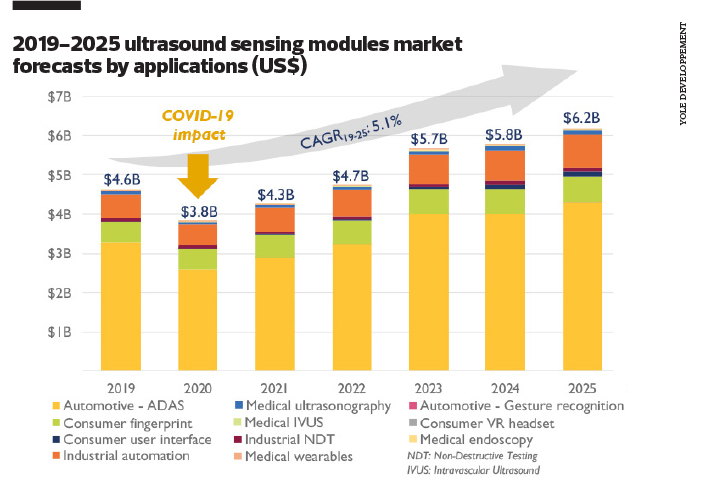
Essentially, ultrasound sensors convert electrical signals into ultrasonic waves and vice versa. According to global industry analyst Yole Développement’s 2020 Ultrasound Sensing Technologies report, ultrasound sensors are seeing emerging demand due to developments in micromachined ultrasound transducers (MUT) that enable ultrasound sensors to be small and easily integrated into various applications.
The biggest market segment is automotive driver assistance systems. The sensors can also be integrated into virtual reality headsets for gesture recognition applications and fingerprint biometrics, as well as point-of-care ultrasound in the medical sector.
The overall compound annual growth rate for ultrasound sensing technologies from 2019 to 2025 is expected to be at 5.1%, according to the report.
Yole identifies SilTerra as one of the top ultrasound sensing technology providers. It is the only Malaysian company in the report to be listed, alongside companies like Philips and Qualcomm.
“Being a SilTerra-owned-and-patented technology, PMUT has the potential for a huge number of applications such as fingerprint sensors, dental and medical imaging devices, as well as automotive collision sensing. Our hope is this will trigger our Malaysian inventors to develop Malaysian products instead of leaving it to companies in other countries,” says SilTerra CEO Firdaus Abdullah.
PMUT allows SilTerra to build low-power sensors, which are critical for the IoT industry. As it utilises silicon-based technology, it also enables the chips to be smaller, according to the company.
How does it work?
PMUT relies on ultrasound, which are sound waves, to “sense” movements and the environment. Different ultrasound frequencies give rise to different applications. At higher frequencies, ultrasound is used for endoscopic procedures or for prenatal imaging on pregnant mothers.
It can also be used for bio-secure fingerprint sensing, where the sensor can detect if a fingerprint is generated by a person or materials such as play-dough that some people may use to try and trick the device.
At lower frequencies, ultrasound can be used for industrial sensors. For instance, a bottling factory may use sensors to detect if the bottles moving rapidly on a conveyor belt are filled or empty.
“If you reduce the frequency further, you can use it for automotive sensors. For instance, cars have the park assist function. It uses ultrasound beams to sense the distance between the car and other objects and can work in any environment. If you use an optical sensor, the sensitivity will drop when weather conditions are bad,” says Arjun.
Gesture recognition, where one just has to wave one’s hands above a screen to control the device, can also be done through PMUT sensors.
“You create an ultrasound beam with low frequency. When you bring your hand close to the screen and move it, you disturb the ultrasound waves. The system will detect the disturbance and interpret your movements. This has tremendous potential because new devices in the next few decades will be using gesture recognition,” says Arjun.
“Another design is for wireless earbuds. One of our customers is planning to put ultrasound sensors in the earbuds so you can just touch the earbud, and move your fingers up and down to adjust the volume.”
SilTerra is currently working with some customers to incorporate PMUT sensors into products. One of the applications eliminates the buttons on the side of smartphones and replaces them with ultrasound sensors. Users just need to slide their fingers or touch the surface to perform specific functions.
“This converts the side of your phone into a mechanical touchpad that is similar to your keypad. This is extremely attractive for people who play games on their phones and don’t like mechanical buttons. Based on how you move your finger and the speed, the sensor can translate it into specific functions,” says Arjun.
What is the progress?
SilTerra started approaching partners about the PMUT technology last year. Currently, it is being evaluated by six to eight global companies, says Arjun, and SilTerra expects to begin commercialising the products this year.
The company has been developing the PMUT for four years. It is already producing and selling other types of sensors for global clients. Among these are biosensors used in DNA sequencing machines by US-based biosciences company Pacific Biosciences of California, Inc.
SilTerra is a foundry that produces the chips that go into the sensors, which are then incorporated into smartphones, medical equipment, vehicles and other products.
It has to work with clients to develop these products, which are often at the cutting edge of technology. The whole process could take a minimum of two years, says Tan Eng Tong, SilTerra’s vice-president of strategic management.
“There is a whole development process that has to take place after the clients buy sensors from us. For instance, they need to put it in the phone and go through testing, run through focus groups and adjust the software, among others. That is the evolution of innovation,” says Tan.
A turnaround for SilTerra?
Five years ago, SilTerra Malaysia Sdn Bhd realised that it could not follow in the footsteps of the biggest wafer fabrication (fabs) plants in the world, which were developing increasingly larger wafers and thinner linewidths.
Nowadays, the world’s leading fabs can manufacture 300mm (12-inch) wafers, while players like SilTerra produce mostly 200mm (8-inch) ones. Producing larger wafers requires advanced technology and a lot of capital.
“At that time, it made sense for fabs to go in that direction because their chips are used to manufacture the latest mobile phones and computers that need high processing power,” says Arjun Kantimahanti, senior vice-president of technology development at SilTerra.
But SilTerra did not have sufficient capital to do so. Instead, it looked at alternatives, and realised that sensors were the next big source of demand for chips. Sensors were being installed into many items that were previously not connected to the internet.
The chips used for sensors could be manufactured by fabs like SilTerra, as they did not necessarily require thinner linewidths that go to 12 nanometres (nm) and even 2nm, which are typically the domain of 300mm fabs.
“In order to build a mobile phone, you still need chips from the 200mm fabs for the display driver, speaker, mic and other items. From 2000 to 2005, nobody believed that you needed a combination of fabs. But by 2010, people thought differently, as more sensors and photonics came into the picture,” says Arjun.
“If you take any product that is available in the market now, I can bet you that at least 10% of the chips in the product comes from 200mm fabs.”
Tan Eng Tong, SilTerra’s vice-president of strategic management, adds that some of the most innovative sensor designers seek 200mm fabs because they are cheaper.
“There is a whole new set of things that never had electronics in them before. You never needed electronics to check your blood type in the past, for instance. And with IoT (Internet of Things), you want to capture everything from temperature, distance to humidity. You need sensors to do that. These sensors don’t necessarily need technologies from the 300mm fabs,” says Tan.
SilTerra took this path, which it refers to as the “More-than-Moore” strategy. This is a reference to an observation by Intel co-founder Gordon Moore that the number of transistors on a microchip doubles every two years, though the cost of computers is halved. What this means is that we can expect the speed and capability of our computers to increase every couple of years, and we will pay less for them.
Instead of going into markets its better-funded competitors were playing in, the capital-starved company decided to take matters into its own hands and focus on emerging markets such as IoT, data centres, the automotive industry and life sciences.
“We have been working on More-than-Moore technologies for many years, thanks to our strategic partners like Imec. These higher-margin technologies are gradually coming online as we work with start-ups to introduce them. In the meantime, we continue to ship our ‘bread and butter’ core business,” says SilTerra CEO Firdaus Abdullah.
Belgium-based Imec is a global research and development hub in nanoelectronics and digital technologies.
According to the company, SilTerra is now seeing the fruits of its labour. It is already shipping silicon photonics to data centres, and it expects its micro-electromechanical systems (MEMS) and biosensor products to take off this year.
Meanwhile, the higher demand for chips globally has benefited the company. The pandemic triggered demand for laptops and servers, while the US-China trade war resulted in supply chain disruptions.
SilTerra’s fab orders for this year were already filled last December. “We don’t have to do any more sales this year. In fact, we have raised prices, and people are still coming to us,” says Tan.
Who are SilTerra’s partners?
SilTerra Malaysia Sdn Bhd works with many global partners to develop new products. Digital Edge spoke to some of them to understand their relationship with SilTerra.
One of the SilTerra’s longest partnerships is with Imec, the Belgium-based global R&D hub for nano and digital technologies.
The partnership started in 2003 as they engaged in the joint development of solutions and technology transfer. The collaboration was stepped up in 2011 when they began developing specialised technologies together.
In some cases, Imec contributes the design and system and relies on SilTerra’s existing technology. In other times, Imec develops the technology and transfers it to SilTerra.
“The gap in the past was that we could develop prototypes and do low-volume manufacturing at Imec, but we couldn’t ramp up our production to higher volumes. That’s why we partnered with SilTerra,” says Haris Osman, vice-president of Imec.
Since then, Imec and SilTerra have worked on developing image sensors, silicon photonics, some micro-electromechanical systems (MEMS) products and life sciences applications. “This partnership is still ongoing. There are multiple chips that we are transferring or developing with SilTerra that are poised for growth,” he adds.
The piezoelectric micromachined ultrasonic transducers (PMUT), Complementary Metal Oxide Semiconductor (CMOS) image sensing, hyperspectral imaging, microfluidic-based sensors for life sciences and a chip for testing Covid-19 are some examples. The DNA sequencing chip developed by Imec is also being transferred to SilTerra.
“We have the capability to do the design systems, materials and the application. After we develop and modify the product, if the customer wants to ramp up the production quickly in terms of volume, we need to transfer it to a foundry and our foundry of choice is SilTerra,” says Haris.
This is because of their many years of collaboration, adds Maarten Willems, vice-president of Imec. “I think this kind of business only makes sense when it’s a win-win situation for both companies. SilTerra is a small-to-mid sized foundry. It wants to diversify its offering beyond CMOS and that can be done by developing specialised technologies together with Imec through a strong collaboration.”
Other partners
Ian Campbell, CEO of OnScale, a US-based software company, has been working with SilTerra on the commercialisation of SilTerra’s MEMS and CMOS foundry technologies. Campbell says he has also been helping SilTerra’s customers leverage on digital prototyping.
“I’ve worked with several foundries and led efforts to vet foundries for new MEMS and CMOS processes. In my opinion, SilTerra is at the forefront of MEMS and CMOS integration and has a very unique capability that will reduce R&D and manufacturing costs in a number of application areas, such as 5G RFFES, biometric devices and miniaturised ultrasonic imagers,” he adds.
Mario De Miguel Ramos, CEO of Sorex Sensors, a University of Cambridge spin-off company, started working with SilTerra in 2019 on projects related to the industrial production of its MEMS sensors.
“The recent pandemic has made us more aware of how important it is to monitor the environment around us. The only way to capture and monitor it is by using sensors, and MEMS sensors offer significant advantages compared to other available technologies now, especially in terms of size and power consumption,” he says.
“The work that SilTerra is doing in the development and optimisation of techniques to scale MEMS sensors is critical to make them widely available to more users and make MEMS sensors the leading technology in the sensing world.”
Professor Nuria Barniol of Universitat Autònoma de Barcelona started her collaboration with SilTerra in 2013. In 2016, she worked with the company to fabricate high-performance PMUT for imaging and biometric sensors. “We are still in the development phase for the optimisation of these PMUTs,” she says.
Save by subscribing to us for
your print and/or
digital copy.
P/S: The Edge is also available on
Apple's App Store and
Android's Google Play.


